The finals of the 2018 International Advanced Semiconductor Innovation Competition took place in Shunyi district of Beijing recently.
Beijing Laize Optoelectronics Technology, Photon Arithmetic (Beijing) Technology, Suzhou Faytech Microelectronics and five other projects signed contracts with Zhongguancun’s Shunyi Science park on the spot.
 |
|
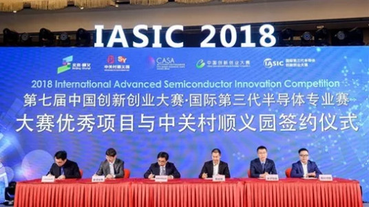
The signing ceremony between outstanding projects in the competition and Zhongguancun's Shunyi science park. [Photo provided to chinadaily.com.cn] |
Zhai Lixin, director of the Zhongguancun Management Committee, spoke highly of the competition. He said that this is not only a competition, but also a platform for cooperation between upstream and downstream industries.
The Zhongguancun Science Park houses over half of the research and education resources in the semiconductor field, and has fostered and gathered a number of innovative enterprises with core technologies and cutting-edge original technological achievements. In Zhongguancun’s Shunyi Park, a whole-industry-chain layout for 3G (third-generation) semiconductors has been formed.
The material market for 3G semiconductors is developing rapidly and has broad prospects. It is an important part of Beijing's high-tech industry and one of the three innovation industrial clusters in Shunyi District.
Currently, Shunyi is making efforts to build an open international public R&D innovation and achievement transformation platform, and accelerate the whole-industry-chain layout of substrates, extensions, chips, devices, modules and leading application enterprises.
The international 3G semiconductor Zhonglian space has been designated a national public space by the Ministry of Science and Technology, and over 50 companies have entered the incubator.
 |
|
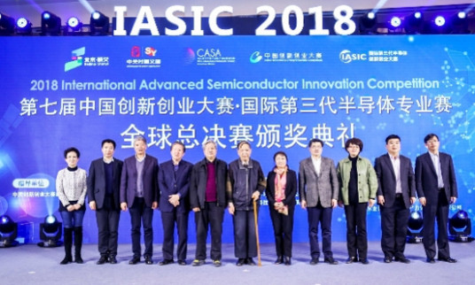
Awarding ceremony of the IASIC 2018 finals [Photo provided to chinadaily.com.cn] |
Meanwhile, the 3G joint innovation base for semiconductor materials and applications was completed this month, covering a total area of 71,000 square meters and accommodating 105 members.
A number of key projects, such as the 13th branch of CEC Group, the Optoelectronics Headquarters of CETC Group, Pinghuboke Semiconductor Chip and Hanergy Mobile Energy Center, have been successively set up, which will form an industrial scale of 100 billion yuan.
Shunyi District has also launched preliminary research and construction plans for the 3G semiconductor industrial agglomeration, compiled an industry development plan for 3G semiconductors and formulated special policies for the industry.
A specialized agency was also set up to strengthen organizational leadership, coordinate financial resources and attract social capital to deepen industrial convergence.