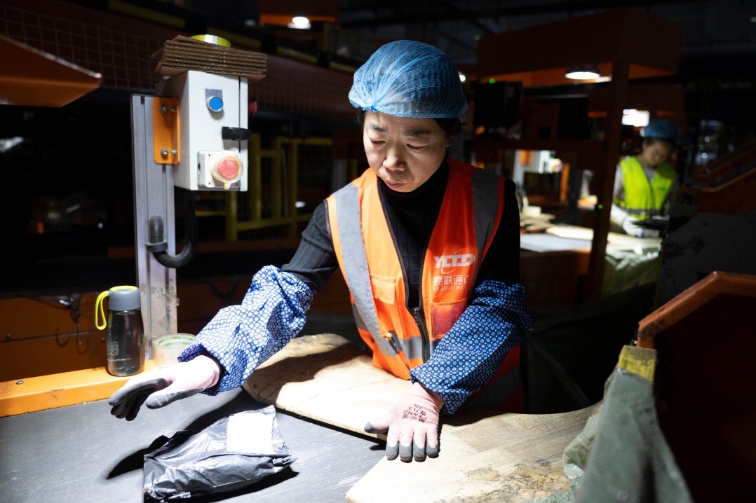
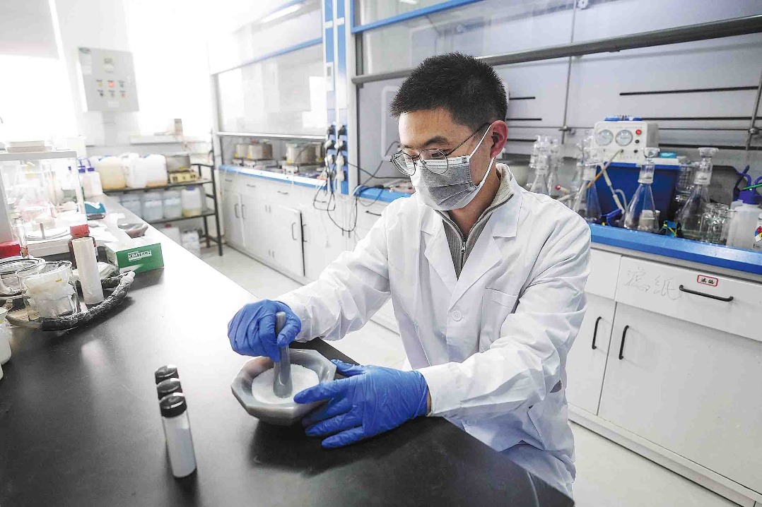
Wuhan firm pioneers laser-cut SiC wafers
By Liu Kun in Wuhan and Wang Songsong |
chinadaily.com.cn |
Updated: 2025-07-29 19:56


Share


Share - WeChat


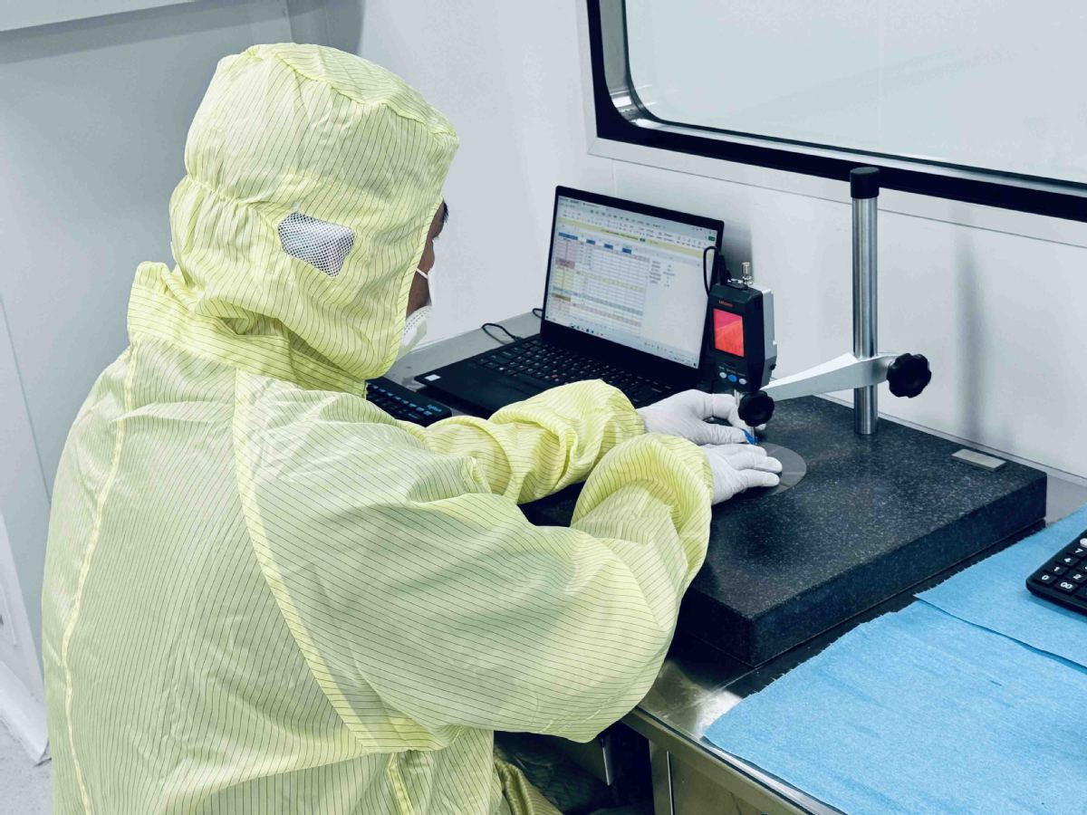
Traditionally, SiC ingots were cut using 100-micrometer diamond wires, a method akin to slicing a carrot. From a 1-cm-thick ingot, only 10 wafers (each 500 μm thick) could be produced, with each cut taking 24 hours and resulting in 50 percent material loss.
In response, Si LAL, the tech firm in Wuhan, has developed laser spalling technology. Instead of "cutting", it uses ultra-precise lasers to focus energy a billion times inside the ingot, altering the SiC structure and "peeling" wafers off layer by layer, similar to how sunlight causes skin to peel.